Successful Use of an Open Source Processor in a Commercial ASIC
by Declan Staunton, Silicon &
Software Systems
Dublin, Ireland
Abstract
Open source IP has been
slow to take off in commercial IC development for very good reasons.
Immaturity of designs, lack of support, licensing and warranty concerns
would normally ensure open source IP cores are not even considered as
solutions. However there are situations, and in the case of the LEON core,
there are solutions that warrant consideration for certain types of
application. Here we describe our experience in using the LEON processor
in a commercial ASIC. Both benefits and drawbacks are described before
concluding that LEON was an excellent solution for this
design.
Introduction
Processor
selection is one of the key design decisions in any SoC development. For
this development there were fewer constraints than would normally be
encountered when choosing a processor. In particular there was no legacy
software or particular operating system that needed to be supported.
Furthermore the vast majority of the logic design was from scratch so
there were no legacy bus interfaces to support. The ASIC was intended for
use in a high volume embedded system. As can be seen from the block
diagram in Fig 1 this was a typical SoC design. The principal requirements
were:
1) Performance: The
initial performance requirements were relatively low but these grew in
time. There were some hard real-time requirements and many firm (meaning
the system would not fail but the user could perceive a slowdown)
real-time requirements
2) Low or no
royalty: As very high volumes were expected this was important
in keeping the unit price low
3) Supervisor & User modes: The
processor would have to support the execution of third party code without
jeopardizing the integrity of the system.
Power consumption was
not a significant concern and while a synthesizable core was preferable
this was primarily due to the unsuitability of the hard cores that were
available for the fabrication process used.
A number of 16 and
32-bit commercial cores were considered before concluding that the LEON
processor offered the best overall solution.
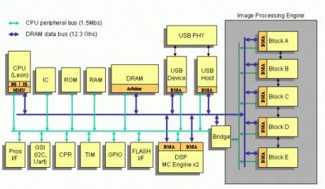
Figure 1: Block diagram of the LEON powered
SoC
The LEON
Processor
LEON is a VHDL implementation of the open standard
(IEEE1754) SPARC V8 architecture [1]. LEON is a highly configurable,
synthesizable, 32-bit core with pre-selectable cache sizes (both I &
D), optional floating point unit and hardware acceleration for multiply
and divide instructions, debug monitor, AMBA AHB [2] interface and support
for a co-processor. Most of the features of LEON can be configured via a
simple GUI which produces a VHDL file of constants that is then referenced
by the other source files. A screenshot of this GUI showing the
configuration options for the Integer Unit is shown in Fig 2.
The
LEON3 processor is available under GPL and commercial license
arrangements. A LGPL version (LEON2) is also available. In fact for most
of the design phase the LEON2 core was used but a late change to the LEON3
core was made for licensing reasons. Despite occurring late in the design
phase, the switchover from LEON2 to LEON3 was not difficult.
A
full software development environment based on the GNU C/C++ compiler is
available for LEON. An instruction set simulator (TSIM) is also available
although this was only rarely used by the IC development team. The LEON
cores and associated IP are available from and supported by Gaisler
Research [3]
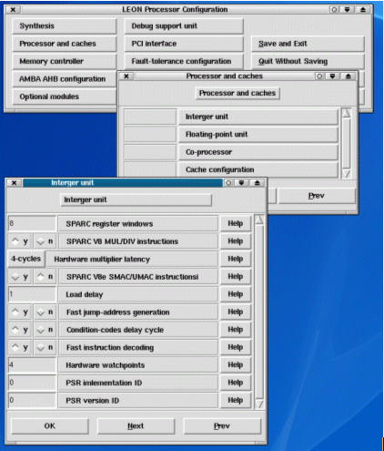
Figure
2: LEON configuration GUI
Using LEON
Familiarisation with
the LEON design was quite straightforward but could have been accelerated
by more complete design documentation and better coding practices. The
code itself was written in a consistent style but the signal and variable
naming were often not very descriptive and comments were scant. Moreover
the extensive use of VHDL records caused problems with some tools and in
some cases a record had to be broken out into its constituent
signals.
The first step in customizing
LEON for our application was the identification of the component entities
we wished to retain and excising these from the LEON deliverable (which
includes bridges, interfaces and peripherals to make it a SoC in its own
right). The components of interest were at the heart of the processor –
the Integer Unit (IU), Cache controllers and AHB interface (there were
some 22 VHDL files required to describe these completely). A testbench was
created to verify the operation of these components in isolation from the
rest of the LEON processor.
The next step
was the creation of a bridge between the LEON AHB interface and the
proprietary bus interfaces to the on-chip DRAM and peripherals. While AMBA
buses were not used elsewhere on the chip their use was advantageous due
to the familiarity of the design team with the standard. With the bridge
in place the LEON CPU core could then be integrated with the remainder of
the ASIC (or more specifically the portions of it that existed at that
time). It was also necessary to select and integrate the correct memories
and register files for the cache data and tag rams and the IU register
file. At a later date it was also necessary to select the appropriate
hardware multiplier and divider circuits. LEON does support memories and
register arrays from a number of foundries (and also FPGA targets) but the
foundry for this ASIC was not supported so this step took some work.
Simple wrappers were also required for each register array / memory.
Modifications
In
order to fulfill the application requirements some modifications and
enhancements were required to the LEON CPU components. All of the LEON
related design work was confined to the CPU subsystem level of hierarchy
depicted in Fig 3 below and this was performed in parallel with the rest
of the ASIC design. Firstly, as the LEON cache controllers refilled
the 256-bit wide cache lines by reading 32 bits at a time and the on-chip
DRAM produced 256-bit lines for every read, it was highly inefficient to
read the same DRAM line 8 times in order to refill a line in the LEON
caches. By making a few changes to both the instruction and data cache
controllers and cache memories it was possible to refill the entire cache
line with the 256 bits yielded by the DRAM read thus reducing the number
of DRAM reads required from 8 to 1.
The most significant
enhancement was the addition of a Memory Management Unit (MMU). Code is
executed on the processor in either supervisor or user mode and the
application required strict enforcement of security rules to ensure user
mode code was restricted in its operation. The primary function of the MMU
was the protection of supervisor mode code and data from user mode
accesses. The MMU was simpler than conventional MMUs in that it did not
feature a Translation Lookaside Buffer (TLB), although it did implement
the memory map for the IC. It is not compatible with the SPARC Reference
MMU specification [4]. The MMU allowed the DRAM address space to be split
into up to 8 regions with each region having programmable access
permissions and start / stop boundaries. The programmable registers
controlling the MMU could of course only be accessed when executing code
in supervisor mode.
Access control for the on-chip peripherals was
distributed i.e. the access control signals were propagated to each
peripheral and each peripheral could accept or reject an access depending
on the permissions of the access and the peripherals settings (this was
often determined on a register by register basis). In addition to
controlling access to the DRAM and peripherals the MMU also included the
AHB to proprietary bus bridges for the DRAM data bus and the CPU
peripheral bus, a write buffer and a bus timeout function to avoid
possible bus hangs.
The purpose of the write buffer was to improve
write performance to minimize the impact of register window over /
underflows. Register windows are a feature of SPARC processors and can
allow fast context switching between tasks. However when a register window
over / underflow occurs the worst case context switch time may become
prohibitive for real-time applications. A small posted write buffer was
added which combined a number of CPU writes into a single write to the
wide DRAM. This was found to improve write performance significantly
(particularly for the sequential writes that are characteristic of window
over / underflow handling) at the cost of complicating the design to
ensure data coherency was upheld in all situations.
Further
modifications were made to the data cache to enforce user / supervisor
data security. Code is executed on the processor in either supervisor or
user mode and the application required strict enforcement of security
rules to ensure user mode code was restricted in its operation. Extra tag
bits and logic were added to the data cache to ensure user mode code could
not retrieve supervisor data from the data cache (this was possible with
the basic LEON design) and the MMU enforced the security of supervisor
mode code and data outside of the caches.
After a reset, the
processor starts executing code from address #00000000. In order to assist
with software error handling (e.g. null pointer de-referencing) all
accesses to the bottom four word locations (i.e. #00000000 to #0000000C)
were trapped by the MMU unless they were made by the reset handler. In all
there were six different conditions introduced that could be trapped by
the MMU to protect the integrity of the system.
These
customisations were made while preserving all of the existing LEON
functionality i.e. no previous LEON functionality was compromised by the
enhancements. While this required a little more design and verification
effort it offered increased confidence in the modified
design.
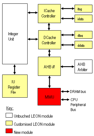
Figure 3: CPU subsystem block
diagram
Integration
As previously
mentioned integration of LEON with the remainder of the chip was mostly a
matter of choosing the correct technology specific macros (i.e. SRAMs,
register arrays, multiplier etc) and then connecting it together. Because
the CPU peripherals had been verified using a bus functional model of the
CPU peripheral bus prior to integration they all worked first time with
the real CPU. One issue that did require some attention during integration
was endianness. SPARC, and therefore LEON, is a big endian architecture
but the rest of the system was little endian. Thus, when data was shared
between the CPU and other blocks (some of which had DMAs with byte-write
capability) careful thought was needed to ensure that bytes were not
swapped around incorrectly. These scenarios were also subjected to
significant directed testing to ensure everything was correct. Where
endianness coherency could not be handled by hardware the need for byte
swapping in software was clearly flagged to the software
developers.
Verification
A number of different
approaches were used to verify the functionality and integration of the
CPU within the ASIC including RTL verification, behavioural modeling in C
and VHDL, external certification of the processor and FPGA emulation.
Unfortunately a complete discussion of the verification strategy used is
outside the scope of this paper. The primary approach for testing the
functionality of the CPU (and in particular the customizations of the LEON
components) was at the subsystem level. This level consisted of all the
CPU subsystem components shown in Fig 3, the Interrupt Controller (this
was a new design rather than the LEON interrupt controller), ROM, RAM,
DRAM arbiter and a behavioural model for the DRAM. Tests were developed
using C and assembly language, compiled using the GNU toolkit available
with LEON and then post processed into appropriately formatted memory
images by perl scripts. A VHDL testbench performed the necessary stimulus
generation and signal monitoring.
LEON modules that were
customized were subjected to full functional verification (i.e. not just
the changes were tested). As the original LEON tests that formed part of
the release were not considered rigorous enough for production silicon
extra effort was expended to ensure satisfactory verification coverage,
particularly of the cache controllers.
Over the course of the
development a number of minor bugs in the LEON design were uncovered by
the verification which were promptly fixed by Gaisler Research. The
success of the verification is best demonstrated by the fact that the
silicon worked first time upon return from the fab without a single
bug.
FPGA Emulation
A significant software development was required to generate
the ROM image and further post-boot downloadable code. While there is an
instruction level simulator (TSIM) available for the LEON processor it
could not model the modifications made to the LEON modules or the other
on-chip components particular to this design. FPGA emulation was clearly
the best solution especially as it also provided an additional layer of
functional verification.
An off the shelf third party board based
on a Xilinx Virtex-II 6000 FGPA was chosen for its large FPGA and short
lead time. Retargeting the LEON modules to the FPGA was straightforward as
Xilinx FPGAs were already supported as a target technology in the LEON
code. Two additional LEON modules were implemented on the FPGA which would
not be present on the ASIC – the Debug Support Unit (DSU) and a UART.
These were required to facilitate software debug and communication with a
host PC.
S3’s GNAT (General-purpose Native jtAg Tester) [5][6]
module was used as part of the FPGA development environment. This module
allows access to the FPGA logic (including ROM / RAM and I/Os) via its
JTAG port. When used in conjunction with VNC [7] full remote control, even
from other sites, of the FPGA board was possible. This allowed the ROM
contents to be updated, the processor reset and onboard LEDs and internal
registers to be monitored all without having to go to the
lab.
Benefits
Outside
of the obvious cost savings one of the primary benefits of using LEON was
the ease with which its capabilities could be augmented as the
requirements grew. This was a significant benefit because, as with all
developments, requirements did change. Initially a cacheless Integer Unit
was to be sufficient but this evolved into a final configuration with 1 kB
I & D caches with the enhancements referred to earlier and hardware
support for the SPARC multiply, multiply and accumulate, and divide
instructions. As the entire source code was available for the extra LEON
features from the very beginning the new features could be turned on
easily and quickly without the need for further dialog (or negotiation)
with the supplier. Indeed once the simulation and synthesis environments
had been set-up simple ‘what-if’ analyses could be easily achieved by
choosing different configuration options with the GUI referred to earlier
and executing our makefile based flow.
Access to the source code
and the freedom to modify it proved very useful not only in performing the
customizations described but also during debug as it was possible to tease
out detailed functionality and to obtain a more complete understanding of
certain behaviours. Without this freedom to modify the core the same
degree of performance improvement would not have been possible.
Furthermore if similar functionality was designed into the non-CPU logic
its complexity, and the probability of a error, would have been increased.
LEON has been designed with direct support for a number of
fabrication technologies (including FPGA) and porting it to a new
technology was not difficult. The code synthesized cleanly and posed no
problems in physical design.
Finally the commercial support
provided by Gaisler Research for the duration of the development was
excellent. We enjoyed a direct interface to the engineers who designed the
core and they were always prompt and accurate in their
responses.
Drawbacks
The coding style used
for LEON required some familiarisation and the lack of comments and
detailed design documentation hampered progress from time to time. The
widespread use of records also caused problems for some CAD tools
(although these may have been addressed by the tool vendors by now). There
were also a number of new releases of the LEON database which fortunately
had little effect on our development – this was because the modules we
were using in our design were only occasionally modified in these new
releases.
Other embedded applications, especially those with
significant real-time requirements, may not find LEON such a good solution
as the use of register windows makes context switching times difficult to
predict and poor in the worst case. Furthermore the register file for the
IU is large – a 144 x 32, 3-port register array was required in our
implementation which used the standard configuration of eight register
windows.
While the software support for LEON is increasing all the
time (a Linux port is now available) careful consideration should be given
to both legacy (as porting may be non-trivial) and new software
requirements. This was not a problem in our application.
While the
code itself has been used and refined many times the testcases that formed
part of the releases used in our development were not comprehensive enough
for an ASIC tapeout. Supplementary testing was required in our
case.
Conclusion
Processor selection is
one of the most important decisions to be made in developing a SoC. When
faced with a clean-sheet design the LEON core is certainly worthy of
serious consideration. The overall quality of the LEON offering is broadly
equal to, and often better than, that of other commercial IP blocks.
While it could be used without any modifications the possibilities for
customization are powerful. Access to the source code, and the ability to
modify it, allowed us to customize the core to our requirements rather
than complicate the logic external to the core. This enabled us to achieve
better performance, better verification and a higher quality design with
zero defects. While LEON may not be as widely suitable as the market
leading processor cores, it proved to be an excellent choice for this
design and doubtless will prove to be so for many others.
References
[1] http://www.us.design-reuse.com/exit?url=http://www.sparc.com/standards.html
[2]
http://www.us.design-reuse.com/exit?url=http://www.arm.com/products/solutions/AMBA_Spec.html
[3]
http://www.us.design-reuse.com/exit?url=http://www.gaisler.com
[4]
SPARC V8 Architecture Manual, Appendix H
[5] http://www.us.design-reuse.com/exit?url=http://www.s3group.com/system_ic/gnat/
[6]
http://www.us.design-reuse.com/exit?url=http://www.xilinx.com/publications/xcellonline/xcell_53/xc_jtag53.htm
[7]
http://www.us.design-reuse.com/exit?url=http://www.realvnc.com,
http://www.us.design-reuse.com/exit?url=http://www.tightvnc.com
 |
| |
Contact Silicon & Software Systems (S3)
|
| |
list: -1137508565.42 seconds
detail:
0.000471115112305 seconds
prov: 0.000668048858643 seconds
end_new
|